NAND gate
The inverse of AND, and enough to build everything else.
NAND gate truth table
| a | b | Q |
|---|---|---|
| 0 | 0 | 1 |
| 0 | 1 | 1 |
| 1 | 0 | 1 |
| 1 | 1 | 0 |
At a glance
- Boolean expression
- ¬(a ∧ b)
- Engineering notation
- (a · b)'
- Inputs
- Two or more
- Output is high when
- any input is low
NAND gate symbol
The ANSI NAND symbol is the AND shape with a bubble on the output. The bubble means inversion, so the symbol reads as AND followed by NOT. The IEC version is the AND rectangle, labelled &, with the same bubble on its output. The logic gate symbols page draws all seven gates side by side in both standards.
How the NAND gate works
A NAND gate outputs 0 only when all of its inputs are 1, and 1 in every other case. It is an AND gate with the output inverted, which is where the name comes from: Not AND.
NAND is functionally complete: every other gate can be built from NAND gates alone, so an entire processor could in principle be made of nothing else. That is not just a curiosity. In CMOS a NAND and a NOR both take four transistors, but the NAND puts its series devices on the fast side and its slow ones in parallel, so for the same drive strength it ends up smaller and quicker. That makes NAND one of the cheapest gates a chip can use, so logic is often mapped onto it; only the inverter, at two transistors, is smaller still.
3-input NAND gate truth table
A 3-input NAND gate is the inverse of a 3-input AND: its output is 0 only when all three inputs are 1. It is not the same as feeding one 2-input NAND into another, because the first inversion gets carried into the second gate. To widen a NAND from 2-input parts, AND the first two inputs and feed that into a NAND with the third.
| a | b | c | Inputs at 1 | Q |
|---|---|---|---|---|
| 0 | 0 | 0 | 0 | 1 |
| 0 | 0 | 1 | 1 | 1 |
| 0 | 1 | 0 | 1 | 1 |
| 0 | 1 | 1 | 2 | 1 |
| 1 | 0 | 0 | 1 | 1 |
| 1 | 0 | 1 | 2 | 1 |
| 1 | 1 | 0 | 2 | 1 |
| 1 | 1 | 1 | 3 | 0 |
Two 2-input NAND gates in a chain, !(!(a & b) & c),
do not give this table:
they differ from it on rows 001, 011, 101 and 111,
and work out to
(a & b) | !c. From 2-input parts, the 3-input gate is
!((a & b) & c).
NAND compared with the other gates
The same four input rows through every gate, with the NAND column highlighted. NOT has only one input, so its column is NOT a and ignores b.
| a | b | AND | OR | NAND | NOR | XOR | XNOR | NOT a |
|---|---|---|---|---|---|---|---|---|
| 0 | 0 | 0 | 0 | 1 | 1 | 0 | 1 | 1 |
| 0 | 1 | 0 | 1 | 1 | 0 | 1 | 0 | 1 |
| 1 | 0 | 0 | 1 | 1 | 0 | 1 | 0 | 0 |
| 1 | 1 | 1 | 1 | 0 | 0 | 0 | 1 | 0 |
- NAND is the exact opposite of AND on every row.
- NAND and NOR agree when the two inputs are equal, and differ on 01 and 10, where NAND gives 1 and NOR gives 0.
Building the NAND gate from other gates
Each of these is equivalent to the NAND gate. Paste any of them into the simulator with ctrl+E to see the circuit.
| Construction | Expression | Equals |
|---|---|---|
| NOT from NAND | !(a & a) | !a |
| AND from NAND | !(!(a & b) & !(a & b)) | a & b |
| OR from NAND | !(!(a & a) & !(b & b)) | a | b |
| De Morgan form | !a | !b | !(a & b) |
NAND gate transistor circuit
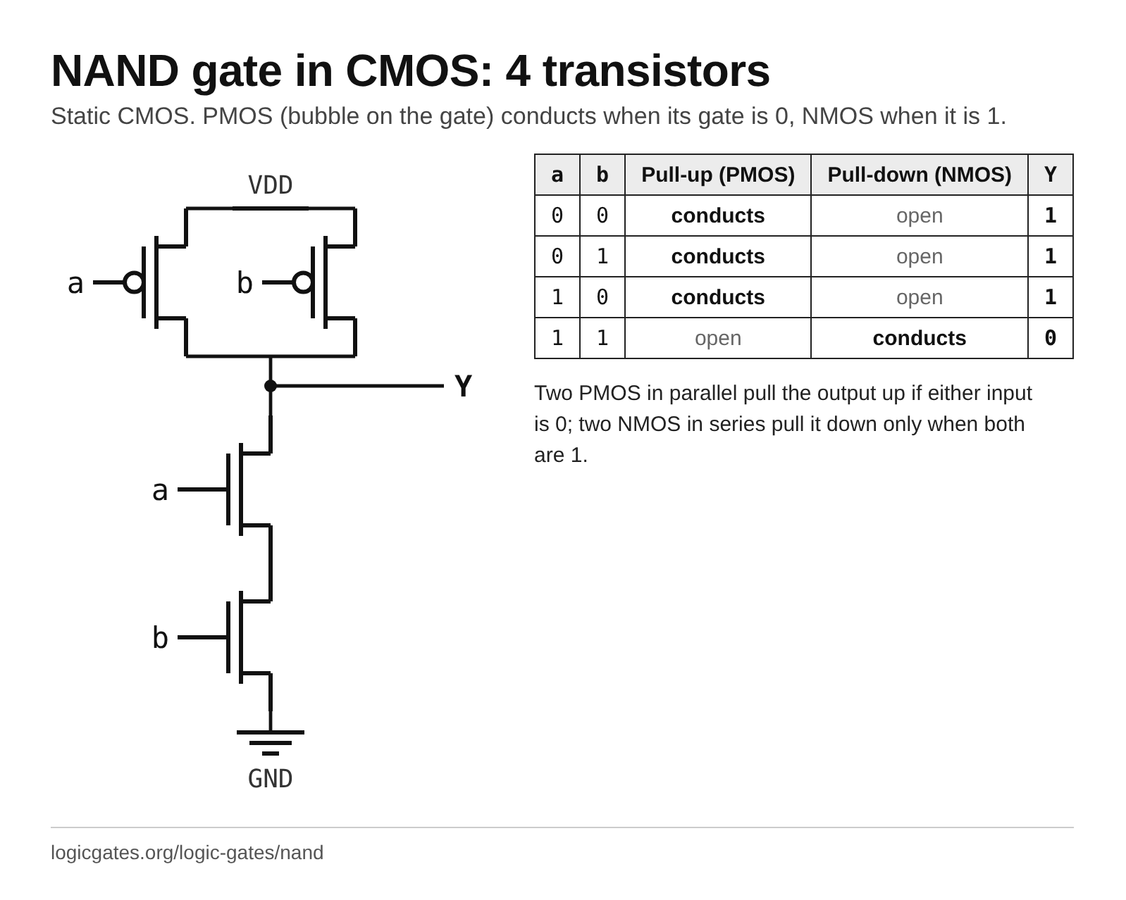
In static CMOS, the textbook NAND gate is a handful of transistors. Toggle the inputs to see which ones switch on and which network connects the output to the supply or to ground.
The pull-up network conducts (the PMOS transistors driven by a and b are on) and the pull-down network is open, so Y is connected to VDD and is 1.
Two PMOS in parallel pull the output up if either input is 0; two NMOS in series pull it down only when both are 1. PMOS transistors, drawn with a bubble on the gate, conduct when their gate is 0; NMOS conduct when it is 1.
NAND gate chip: the 7400 pinout
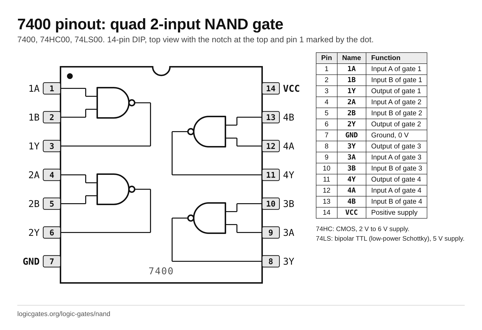
To build with real parts, the NAND gate comes four to a package in the 7400 series. The 7400 is a quad 2-input NAND gate.
7400, 74HC00, 74LS00: quad 2-input NAND gate, 14-pin DIP
| Pin | Name | Function |
|---|---|---|
| 1 | 1A | Input A of gate 1 |
| 2 | 1B | Input B of gate 1 |
| 3 | 1Y | Output of gate 1 |
| 4 | 2A | Input A of gate 2 |
| 5 | 2B | Input B of gate 2 |
| 6 | 2Y | Output of gate 2 |
| 7 | GND | Ground, 0 V |
| 8 | 3Y | Output of gate 3 |
| 9 | 3A | Input A of gate 3 |
| 10 | 3B | Input B of gate 3 |
| 11 | 4Y | Output of gate 4 |
| 12 | 4A | Input A of gate 4 |
| 13 | 4B | Input B of gate 4 |
| 14 | VCC | Positive supply |
- 74HC: CMOS, 2 V to 6 V supply.
- 74LS: bipolar TTL (low-power Schottky), 5 V supply.
NAND gate examples
Everyday and engineering things that follow the NAND rule.
- A "door open" warning light that stays lit until every door reports shut: the light is on when not all the doors are closed, which is a NAND of the door sensors.
- NAND flash, the memory in SSDs and USB sticks, is named after its layout: its cells are connected in series, like the transistors in a NAND gate's pull-down network. It is a name for the wiring; the memory array is not built from NAND gates.
- The 7400, the first part number in the classic 7400 logic family, holds four 2-input NAND gates in one package.
- The Nand to Tetris course builds a working computer, step by step, starting from nothing but the NAND gate.
Where the NAND gate is used
- Building any other gate, which is why NAND is the workhorse of real logic families.
- Cross-coupling two NAND gates gives an SR latch, the simplest circuit that remembers a bit.
- Replacing an AND followed by a NOT with a single, faster gate.
NAND gate reference card
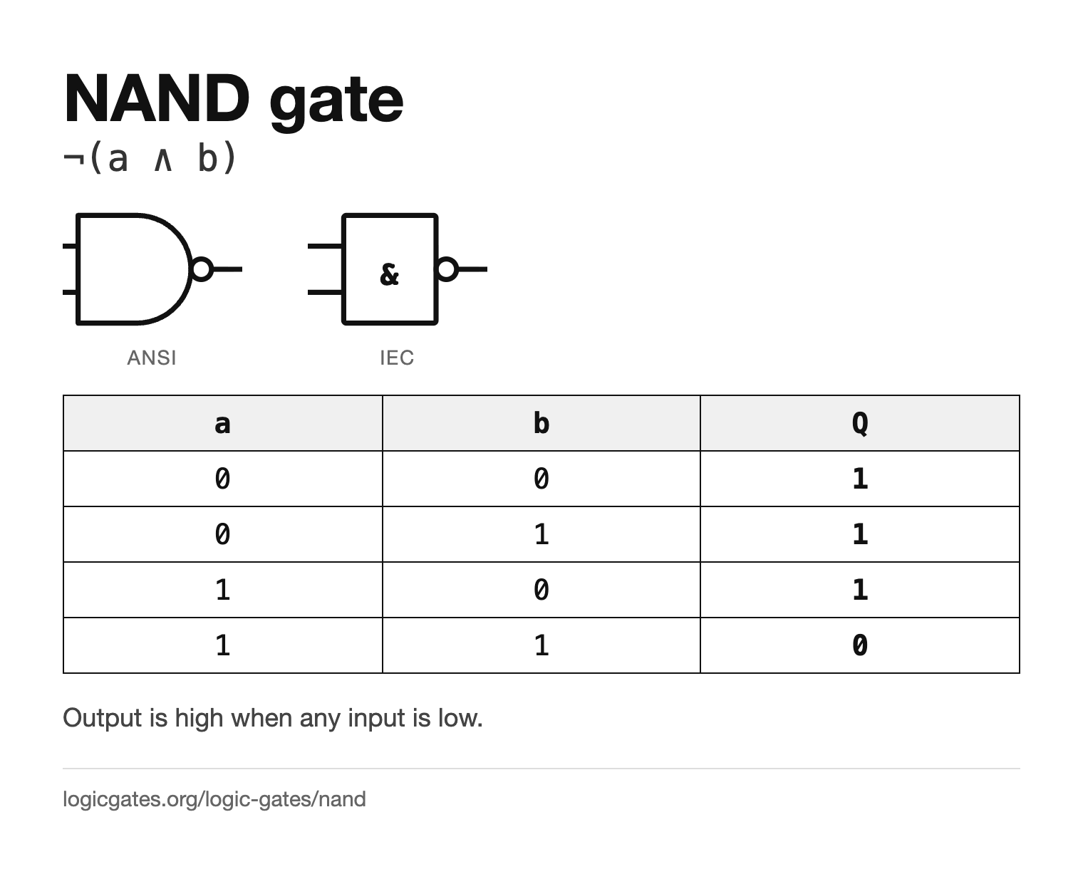
The symbol in both standards and the truth table on one image, for notes or a slide.
 Click to download the NAND reference card
In the simulator
NAND is in the Logic menu and takes a configurable number of inputs. Try rebuilding a half adder from NAND gates alone; it takes five.
Questions about the NAND gate
What does a NAND gate do?
It outputs 0 only when all of its inputs are 1, and 1 in every other case. It is an AND gate followed by a NOT, combined into one gate.
What is the symbol for a NAND gate?
The AND symbol with a small circle, the inversion bubble, on the output. In the IEC style it is a rectangle labelled & with the bubble on its output.
Why is NAND called a universal gate?
Because NOT, AND and OR can all be built from NAND gates alone, and those three are enough to express any boolean function. So any circuit at all can be rewritten using only NAND gates. NOR is universal for the same reason.
What is the difference between NAND and NOR?
NAND is an inverted AND: it outputs 0 only when every input is 1. NOR is an inverted OR: it outputs 1 only when every input is 0. So NAND is 1 on three of its four rows and NOR on just one. Invert every input and the output of a NAND and you get a NOR, which is De Morgan's law in gate form. Both are universal.
How do you make a NOT gate from a NAND gate?
Tie both inputs together, or hold one input high. A NAND with both inputs fed by the same signal outputs the inverse of that signal.