NOT gate
Outputs the opposite of its single input.
NOT gate truth table
| a | Q |
|---|---|
| 0 | 1 |
| 1 | 0 |
At a glance
- Boolean expression
- ¬a
- Engineering notation
- a'
- Inputs
- One
- Output is high when
- its single input is low
NOT gate symbol
The ANSI symbol is a triangle pointing towards the output, with a small circle, the bubble, on its tip. The triangle alone is a buffer, which passes its input through unchanged; the bubble is the part that means inversion. The IEC symbol is a rectangle labelled 1, with the same bubble on the output. The logic gate symbols page draws all seven gates side by side in both standards.
How the NOT gate works
A NOT gate, also called an inverter, has one input and one output. It turns 1 into 0 and 0 into 1. Inverting twice gets you back where you started, which is the double negation law.
It is the only gate that does not combine anything. Everything else on this page merges two or more signals; the inverter just flips one. That makes it the piece that turns AND into NAND, OR into NOR, and a positive condition into a negative one.
NOT compared with the other gates
The same four input rows through every gate, with the NOT column highlighted. NOT has only one input, so its column is NOT a and ignores b.
| a | b | AND | OR | NAND | NOR | XOR | XNOR | NOT a |
|---|---|---|---|---|---|---|---|---|
| 0 | 0 | 0 | 0 | 1 | 1 | 0 | 1 | 1 |
| 0 | 1 | 0 | 1 | 1 | 0 | 1 | 0 | 1 |
| 1 | 0 | 0 | 1 | 1 | 0 | 1 | 0 | 0 |
| 1 | 1 | 1 | 1 | 0 | 0 | 0 | 1 | 0 |
- NOT a differs from NAND only on row 10, and agrees with it whenever a and b are equal. That is why a NAND with both inputs tied together is an inverter.
- NOT a differs from NOR only on row 01, so a NOR with its inputs tied together is an inverter too.
Building the NOT gate from other gates
Each of these is equivalent to the NOT gate. Paste any of them into the simulator with ctrl+E to see the circuit.
| Construction | Expression | Equals |
|---|---|---|
| From a NAND gate | !(a & a) | !a |
| From a NOR gate | !(a | a) | !a |
| From XOR with a 1 | a ^ 1 | !a |
NOT gate transistor circuit
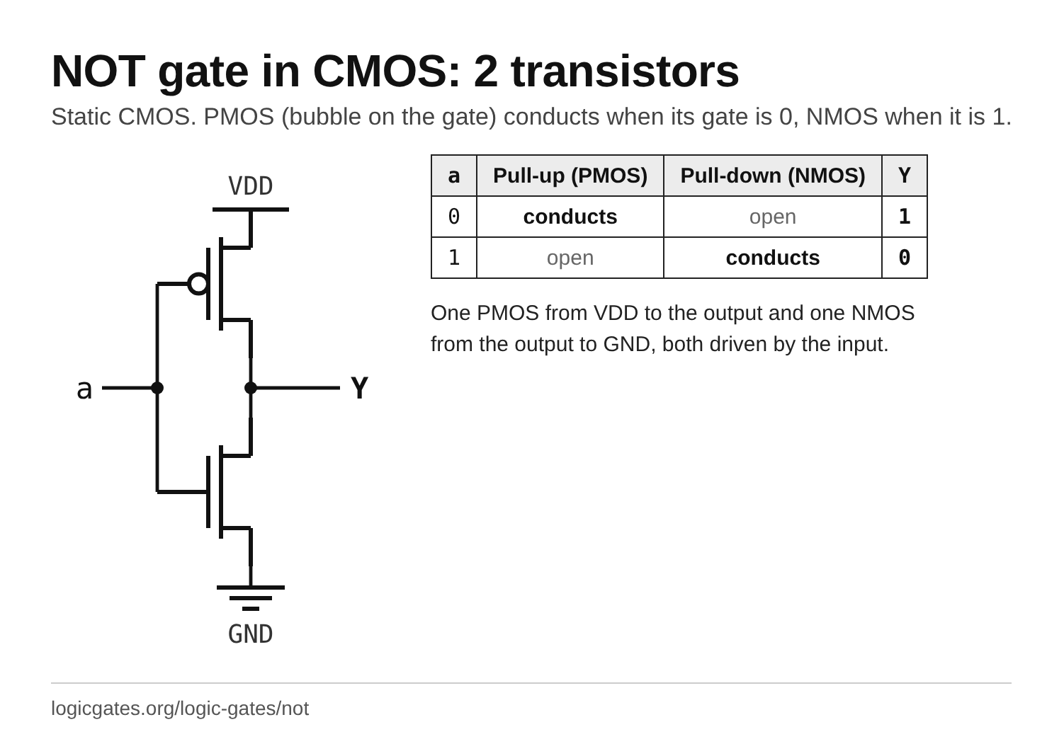
In static CMOS, the textbook NOT gate is a handful of transistors. Toggle the inputs to see which ones switch on and which network connects the output to the supply or to ground.
The pull-up network conducts (the PMOS driven by a is on) and the pull-down network is open, so Y is connected to VDD and is 1.
One PMOS from VDD to the output and one NMOS from the output to GND, both driven by the input. PMOS transistors, drawn with a bubble on the gate, conduct when their gate is 0; NMOS conduct when it is 1.
NOT gate chip: the 7404 pinout
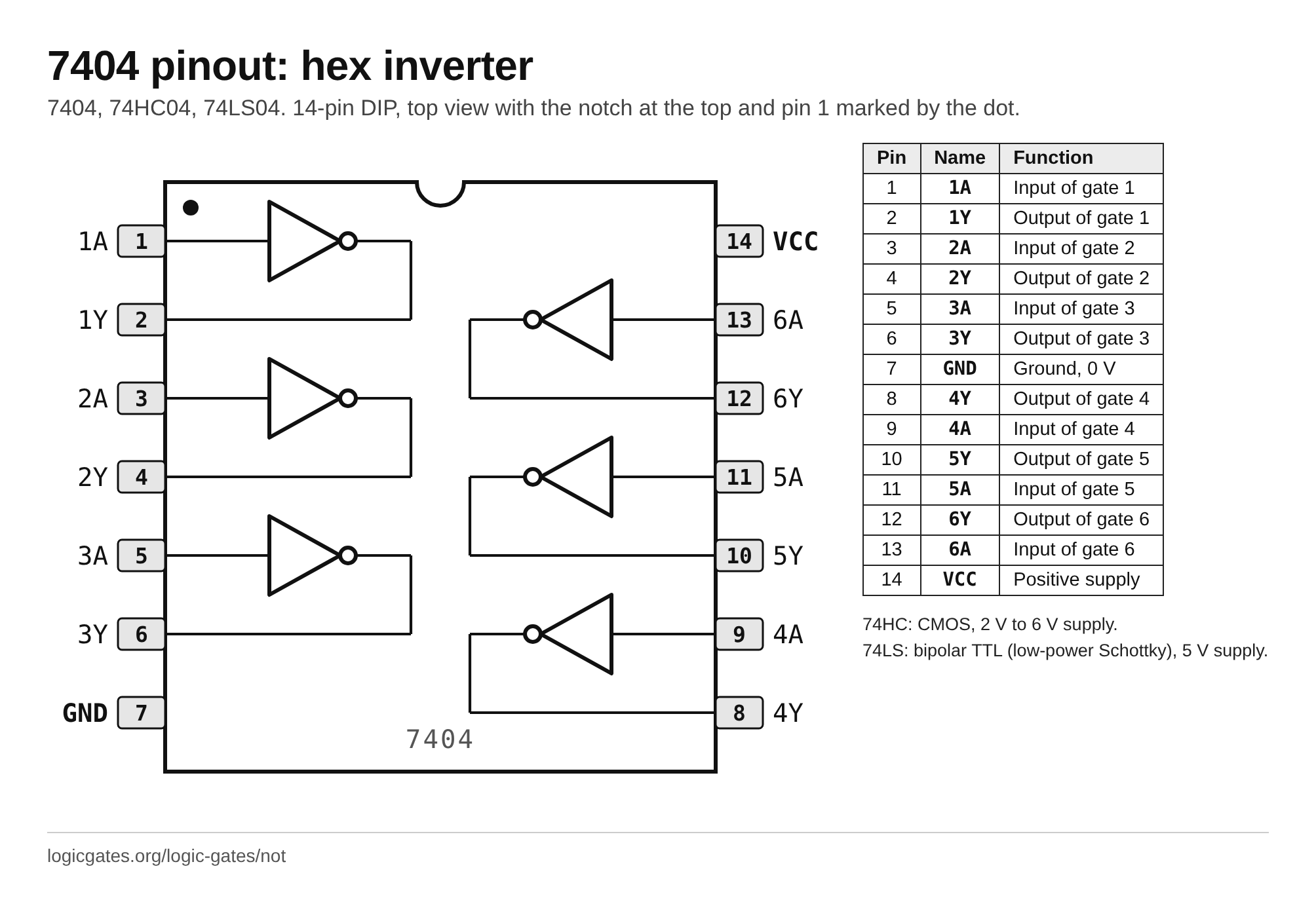
To build with real parts, the NOT gate comes six to a package in the 7400 series. The 7404 is a hex inverter.
7404, 74HC04, 74LS04: hex inverter, 14-pin DIP
| Pin | Name | Function |
|---|---|---|
| 1 | 1A | Input of gate 1 |
| 2 | 1Y | Output of gate 1 |
| 3 | 2A | Input of gate 2 |
| 4 | 2Y | Output of gate 2 |
| 5 | 3A | Input of gate 3 |
| 6 | 3Y | Output of gate 3 |
| 7 | GND | Ground, 0 V |
| 8 | 4Y | Output of gate 4 |
| 9 | 4A | Input of gate 4 |
| 10 | 5Y | Output of gate 5 |
| 11 | 5A | Input of gate 5 |
| 12 | 6Y | Output of gate 6 |
| 13 | 6A | Input of gate 6 |
| 14 | VCC | Positive supply |
- 74HC: CMOS, 2 V to 6 V supply.
- 74LS: bipolar TTL (low-power Schottky), 5 V supply.
NOT gate examples
Everyday and engineering things that follow the NOT rule.
- A fridge light is switched by a button that the closed door holds in, so the light is on when the door is not closed.
- A dusk-to-dawn outdoor light switches on when its sensor does not see daylight.
- A normally closed stop button carries current until it is pressed, so the circuit is on exactly when the button is not pressed.
Where the NOT gate is used
- Turning an active-low signal into an active-high one, or the other way round.
- Completing a set: AND and OR alone cannot express everything, but add NOT and you can express any boolean function at all.
- Building a ring oscillator, where an odd number of inverters in a loop never settles and oscillates instead.
- Producing the complement of a variable for a sum of products expression.
NOT gate reference card
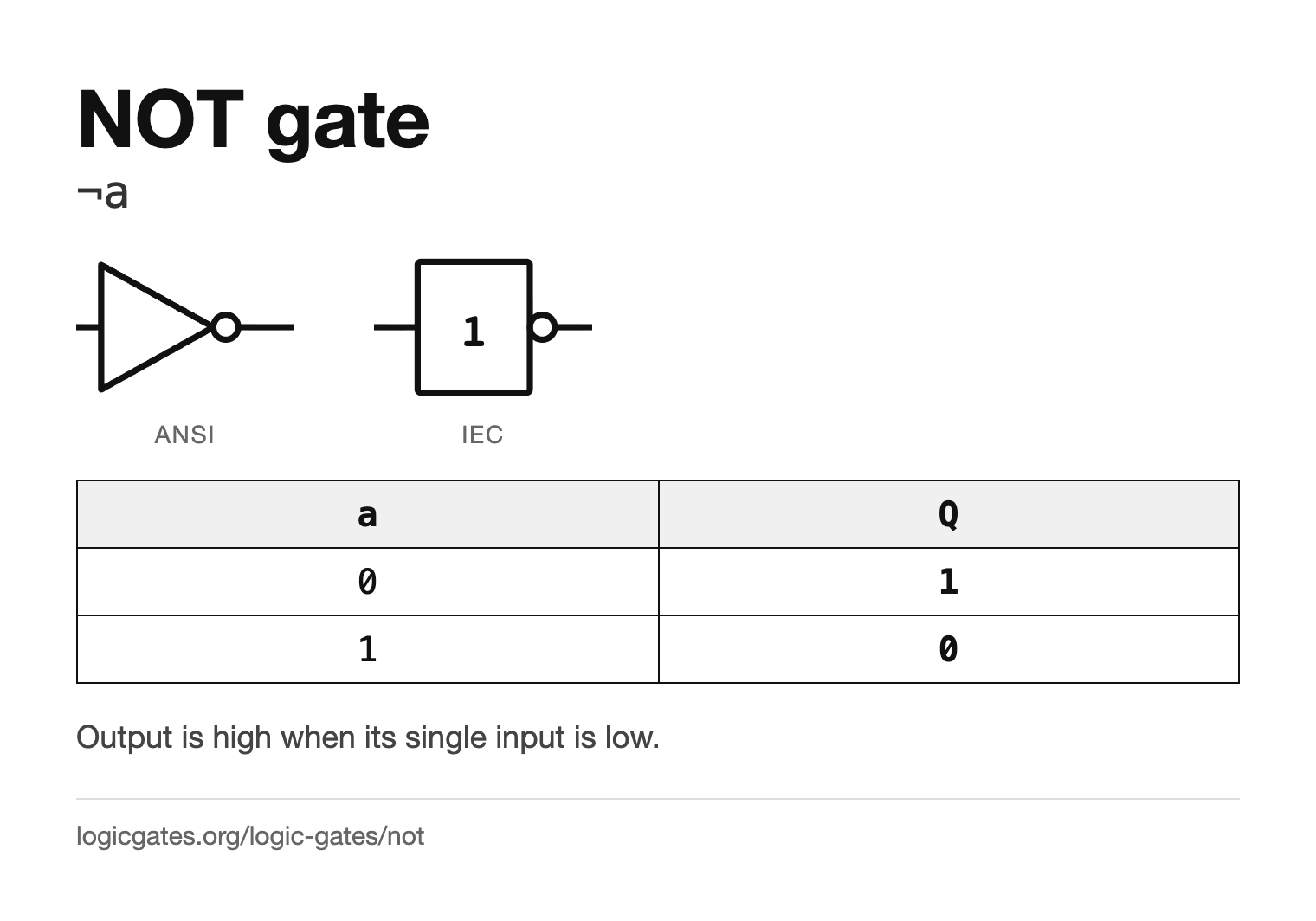
The symbol in both standards and the truth table on one image, for notes or a slide.
 Click to download the NOT reference card
In the simulator
NOT is in the Logic menu. It is the one gate with a fixed single input, so there is no input count to set.
Questions about the NOT gate
What does a NOT gate do?
It outputs the opposite of its single input: 1 becomes 0 and 0 becomes 1.
What is the symbol for a NOT gate?
In the ANSI style it is a triangle with a small circle on its output, the circle being what means inversion. In the IEC style it is a rectangle labelled 1 with the same circle on the output.
Can a NOT gate have two inputs?
No. A NOT gate always has exactly one input. An inverted combination of two signals is a NAND, NOR or XNOR gate.
Why is a NOT gate called an inverter?
Because it inverts its input: the output is always the opposite level. The two names mean the same thing, and in circuit diagrams it is drawn as a triangle with a small bubble on the output, the bubble being the part that means inversion.
What happens if I chain two NOT gates?
You get the original signal back, since inverting twice cancels out. It is not useless though: a pair of inverters is often used as a buffer, to strengthen a weak signal or to add a deliberate delay.